Hardware Connection
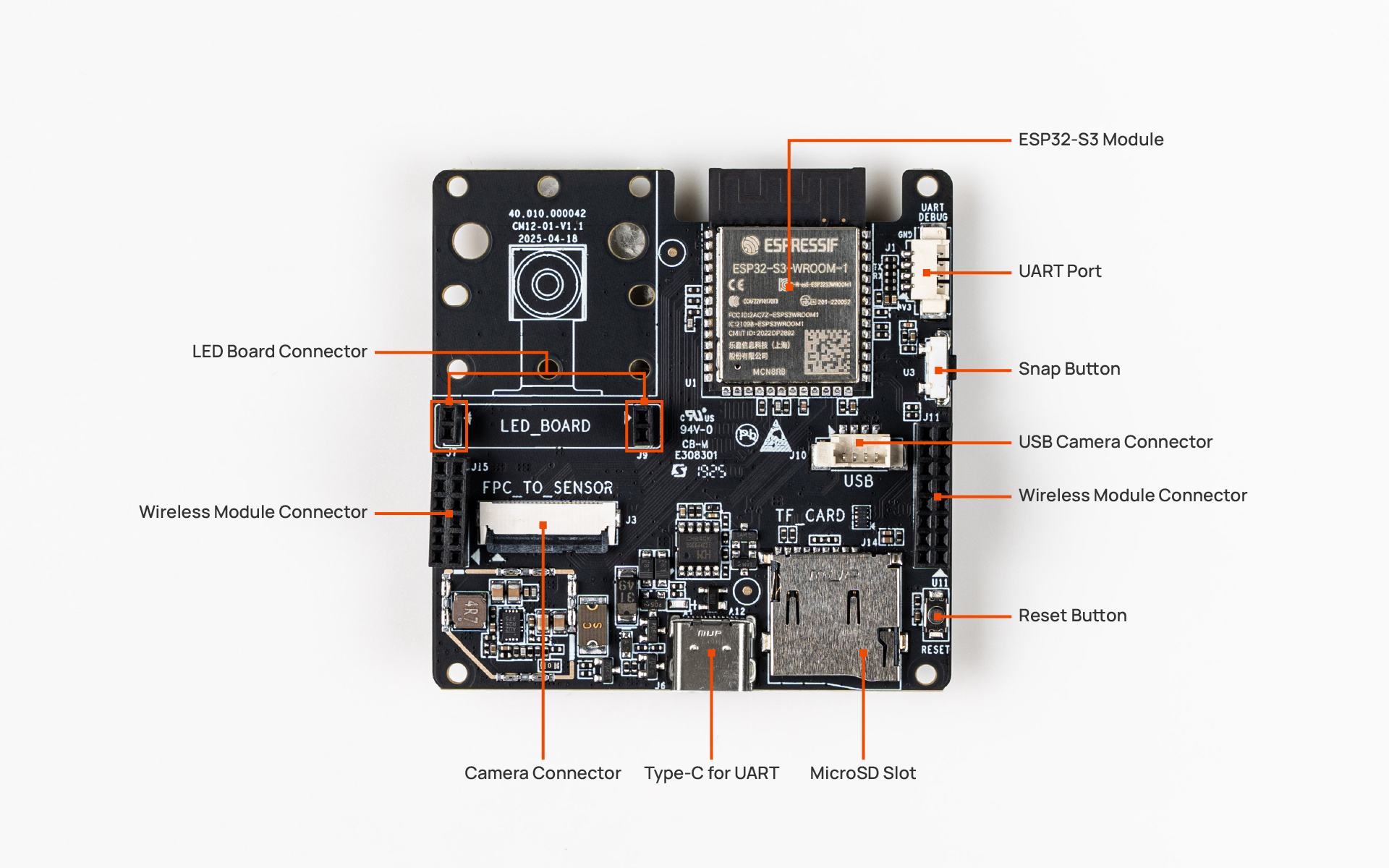
Main Board Interfaces Overview
Top side Interfaces:
- Type-C for UART and Power Supply
- MicroSD Slot
- Reset Button
- Wireless Module Connector
- Sanp Button
- Uart Port for Debug
- USB Camera Connector
- LED Board Connector
- Camera Module Interface
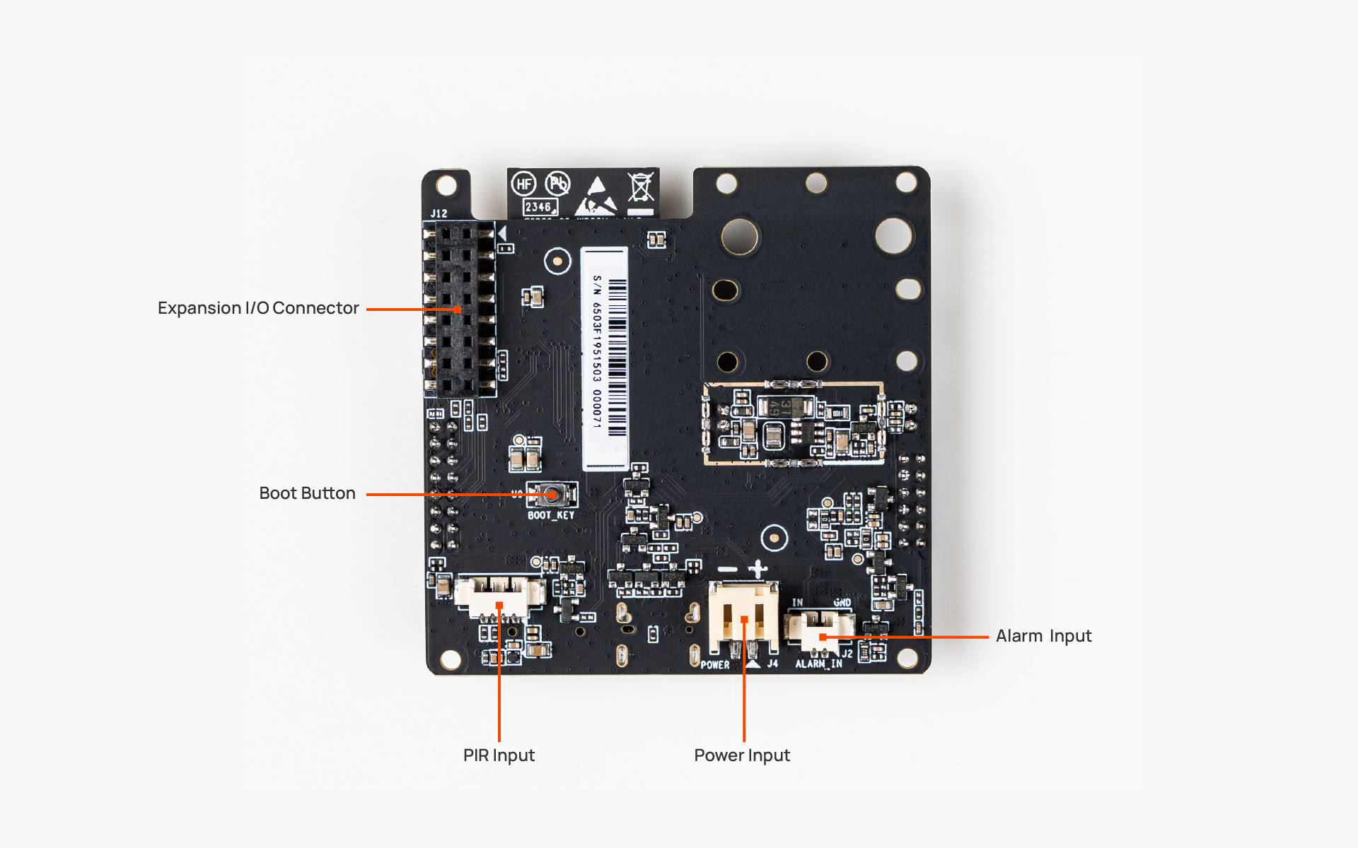
Bottom side Interfaces:
- Power Input Connector
- Alarm Input Connector
- PIR Input Connector
- Expansioin GPIOs, include UART、I2C、SPI、Power Output
- Boot Button
Demo Kit quick start guide
- After unpacking, inspect the Main Board and accessories to ensure they are intact.
- Connect the Camera Module (OV5640 Module or USB Module) to the main board.
- Attach the communication module (Cat-1 or WiFi-Halow) to the main board (optional).
- Connect the debug UART port via the Type-C or 4Pin Wafer connector.
- Supply power through the Type-C port or the power connector.
- After completing the above steps, you may begin the related debugging procedures.
For program and debug, please ref:AI Camera System Flashing
Interfaces description
Peripherals power Ctrl
Before using the camera, ISP, battery level detection, flash, or light sensor, the CAM_PWR pin must be set high to enable their operation. Similarly, the TF_PWR pin must be set high before using the TF card.
| PIN# | Pin Name | Functions | Pin Type | Pull Up/Down | Alternate Function |
|---|---|---|---|---|---|
| 16 | CAM_PWR | GPIO3 | O | PD 10K | |
| 35 | TF_PWR | GPIO42 | O | PD 100K |
PIR GPIOs Defined
| PIN# | Pin Name | Functions | Pin Type | Pull Up/Down | Alternate Function |
|---|---|---|---|---|---|
| 1 | VDD | Power supply | S | ||
| 2 | GND | GND | S | ||
| 3 | Serial_IN | Config Port | I/O/T | GPIO41 | |
| 4 | INT/Dout | AlarmIN | I/O/T | GPIO2 |
16Pin GPIOs Expansion
The 16 pins expansion header provide communication interface like uart, I2C, SPI and GPIOs. Developer can use these interfaces to expand sensor modules like PIR sensor, OLED module as their needed.
| PIN# | Pin Name | Functions | Pin Type | Pull Up/Down | Alternate Function |
|---|---|---|---|---|---|
| 1 | TXD0 | Uart0 TX | I/O/T | PU 10K | GPIO43 |
| 2 | GND | GND | S | ||
| 3 | RXD0 | Uart0 RX | I/O/T | PU 10K | GPIO44 |
| 4 | GND | GND | S | ||
| 5 | GPIO | GPIO41 | I/O/T | ||
| 6 | 5V0 | 5V0 Input | S | ||
| 7 | SPI_MISO | SPI_MISO | I/O/T | GPIO40 | |
| 8 | 3V3 | 3V3 Output | S | ||
| 9 | SPI_CLK | SPI_CLK | I/O/T | GPIO39 | |
| 10 | Alarm_IN | Alarm Input | I | GPIO2,ADC1_CH1 | |
| 11 | SPI_MOSI | SPI_MOSI | I/O/T | GPIO38 | |
| 12 | SPI_CS | SPI_CS | I/O/T | GPIO45 | |
| 13 | GPIO | GPIO19 | I/O/T | USB_D-,ADC2_CH8 | |
| 14 | GPIO | GPIO48 | I/O/T | ||
| 15 | GPIO | GPIO20 | I/O/T | USB_D+,ADC2_CH9 | |
| 16 | GPIO | GPIO46 | I/O/T |
Camera Sensor IOs
Camera Module OV5640 support 8-bit paralle input interface. The IOs of main board config as below
| PIN# | Pin Name | Functions | Pin Type | Pull Up/Down | ESP32-S3 PINs |
|---|---|---|---|---|---|
| 1 | Null | ||||
| 2 | GND | GND | S | ||
| 3 | I2C_SDA | I2C_Data | I/O | PU 4K7 | GPIO4 |
| 4 | AVDD | 2.8V | S | ||
| 5 | I2C_SCL | I2C_Clock | O | PU 4K7 | GPIO5 |
| 6 | CAM_RST | Reset#low | RC circuit | ||
| 7 | CSI_VSYNC | V-Sync | I | GPIO6 | |
| 8 | CSI_PWDN | PD 1K | |||
| 9 | CSI_HSYNC | H-Sync | I | GPIO7 | |
| 10 | DVDD | 1V2 | S | ||
| 11 | DOVDD | 2V8 | S | ||
| 12 | CSI_D7 | Data_Bit7 | I | GPIO16 | |
| 13 | CSI_MCLK | Clock_output | O | GPIO15 | |
| 14 | CSI_D6 | Data_Bit6 | I | GPIO17 | |
| 15 | GND | GND | S | ||
| 16 | CSI_D5 | Data_Bit5 | I | GPIO18 | |
| 17 | CSI_PCLK | Pixel Clock | I | GPIO13 | |
| 18 | CSI_D4 | Data_Bit4 | I | GPIO12 | |
| 19 | CSI_D0 | Data_Bit0 | I | GPIO11 | |
| 20 | CSI_D3 | Data_Bit3 | I | GPIO10 | |
| 21 | CSI_D1 | Data_Bit1 | I | GPIO9 | |
| 22 | CSI_D2 | Data_Bit2 | I | GPIO8 | |
| 23 | Null | ||||
| 24 | Null |
Note: 1. Set the CAM_PWR pin high before use.
Flash and Light Sensor IOs
| PIN# | Pin Name | Functions | Pin Type | Pull Up/Down | ESP32-S3 PINs |
|---|---|---|---|---|---|
| 24 | FLASH_LED | LEDC_PWM | O | PD 100K | GPIO47 |
| 39 | LIGHT_RESISTOR | ADC | A | GPIO1 |
Note: 1. Set the CAM_PWR pin high before use; 2. A light intensity of 0% to 100% corresponds to an output voltage of 0 to 2.5V.
TF Card IOs
| PIN# | Pin Name | Functions | Pin Type | Pull Up/Down | ESP32-S3 PINs |
|---|---|---|---|---|---|
| 31 | CMD | SDIO_CMD | O | PU 10K | GPIO38 |
| 32 | CLK | SDIO_CLK | O | PU 10K | GPIO39 |
| 33 | DAT0 | SDIO_DA0 | I | PU 10K | GPIO40 |
| 34 | CD | SDIO_IRQ | I | PU 1M | GPIO41 |
Note: 1. Set the TF_PWR pin high before use; 2. Please use MMC 1-bit mode protocol driver; 3. Cannot be used simultaneously with WiFi-Halow and 4G Cat1 modules due to pin conflicts.
Other IOs
| PIN# | Pin Name | Functions | Pin Type | Pull Up/Down | ESP32-S3 PINs |
|---|---|---|---|---|---|
| 23 | CFG_KEY | IRQ_IN | I | PU 10K | GPIO21 |
| 22 | BAT_DET | ADC | A | GPIO14 |
Note: 1. Before starting battery level detection, the CAM_PWR pin must be set high; 2. The battery level from 0% to 100% corresponds to a voltage range of 1.8 to 3V.
Communication Module Pins Header defined
Communication Module is mounted on J11 & J15 Pins Header. The J11 16 Pins Header provide related signals. The J15 12 Pins Header only for phsical support. Please note that for IOs sources lack, the IO configuration conflit with some IOs
16 Pins Expansion Header
Detailed information please reference the comparison table.
| PIN# | Pin Name | Functions | Pin Type | Pull Up/Down | ESP32-S3 PINs |
|---|---|---|---|---|---|
| 1 | VCC_IN | Power Output | S | ||
| 2 | 3V3 | 3V3 Output | S | ||
| 3 | VCC_IN | Power Output | S | ||
| 4 | 3V3 | 3V3 Output | S | ||
| 5 | WIFI_PWR_H | Power Enable | I/O/T | GPIO48 | |
| 6 | GND | GND | |||
| 7 | SPI_MOSI | SPI_MOSI | I/O/T | GPIO38 | |
| 8 | SPI_MISO | SPI_MISO | I/O/T | GPIO40 | |
| 9 | SPI_CS | SPI_CS | I/O/T | GPIO45 | |
| 10 | SPI_CS | SPI_CS | I/O/T | GPIO45 | |
| 11 | WIFI_BUSY | Status | I/O/T | GPIO20,USB_D+,ADC2_CH9 | |
| 12 | IRQ | Interrupt | I/O/T | GPIO41 | |
| 13 | GND | GND | |||
| 14 | WIFI_WAKE | Wake_Up | I/O/T | GPIO19,USB_D-,ADC2_CH8 | |
| 15 | SPI_CLK | SPI_CLK | I/O/T | GPIO39 | |
| 16 | WIFI_RST | Reset#low | I/O/T | GPIO46 |
IO Conflict table
If you use the Cat-1 or WiFi-Halow Module,the IOs occupancy by the module should not be used or connected anything on 16 Pins Expansion header.
| PIN# | Pin Name | Functions | Cat-1 Module | WiFi-Halow Module |
|---|---|---|---|---|
| 1 | TXD0 | Uart0 TX | ||
| 2 | GND | GND | ||
| 3 | RXD0 | Uart0 RX | ||
| 4 | GND | GND | ||
| 5 | GPIO | GPIO41 | IRQ | |
| 6 | 3V3 | 3V3 Output | ||
| 7 | SPI_MISO | SPI_MISO | UART_TXD | SPI_MISO |
| 8 | 3V3 | 3V3 Output | ||
| 9 | SPI_CLK | SPI_CLK | UART_RXD | SPI_CLK |
| 10 | Alarm_IN | Alarm Input | ||
| 11 | SPI_MOSI | SPI_MOSI | SPI_MOSI | |
| 12 | SPI_CS | SPI_CS | SPI_CS | |
| 13 | GPIO | GPIO19 | WIFI_WAKE | |
| 14 | GPIO | GPIO48 | CAT1_PWR_H | WIFI_PWR_H |
| 15 | GPIO | GPIO20 | WIFI_RST | |
| 16 | GPIO | GPIO46 | WIFI_BUSY |